研究进展
合肥工业大学梁水保Chip:先进封装硅通孔热-应力耦合驱动的晶粒演化与旋转机制
近日,合肥工业大学梁水保团队以「Unraveling thermomechanical stress-driven grain evolution and rotation in through-silicon vias for advanced packaging」¹为题在Chip上发表研究论文,发展了多场耦合数值框架,以揭示先进封装硅通孔结构中热-应力耦合驱动的晶粒演化和旋转机制。
- 本站发布
- 2026年11月4日
转自 FUTURE 远见
FUTURE | 远见 选编
近日,合肥工业大学梁水保团队以「Unraveling thermomechanical stress-driven grain evolution and rotation in through-silicon vias for advanced packaging」¹为题在Chip上发表研究论文,发展了多场耦合数值框架,以揭示先进封装硅通孔结构中热-应力耦合驱动的晶粒演化和旋转机制。第一作者为Han Jiang,通讯作者为梁水保。Chip是全球聚焦芯片类研究的综合性国际期刊,是入选了国家高起点新刊计划的「三类高质量论文」期刊之一。
随着人工智能和高性能计算的发展,3D集成电路(3D Integrated Circuits,3D IC)对高密度垂直互连提出了更高要求²-³。硅通孔(Through-Silicon Vias,TSV)中的Cu柱在尺寸缩小后往往仅包含少数晶粒,其晶体取向特征与Cu/Si热膨胀失配产生的热应力会显著影响晶粒演化及互连可靠性⁴。因此,揭示热-应力耦合驱动下先进封装TSV中晶粒的长大与旋转机制,对优化TSV微观结构及性能具有重要意义。
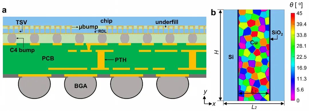
图1 | 3D集成与TSV结构示意图。 a, 高密度3D堆叠芯片及TSV结构;b, 包含不同取向晶粒的TSV结构。
如图1所示,TSV作为3D集成结构中的垂直互连,其内部Cu柱由具有不同晶体取向的晶粒组成。在本工作中,研究者建立了耦合晶界迁移、晶粒旋转与热应力的数值框架,基于Kobayashi–Warren–Carter模型⁵描述TSV中的晶粒形貌与动态演化,并考虑取向相关的应变能影响。研究了退火过程中热应力对TSV微结构演化的影响。如图2所示,结果表明,无热应力时TSV中Cu晶粒主要发生粗化;在热应力作用下,晶粒长大与取向旋转明显增强,并呈现择优取向。
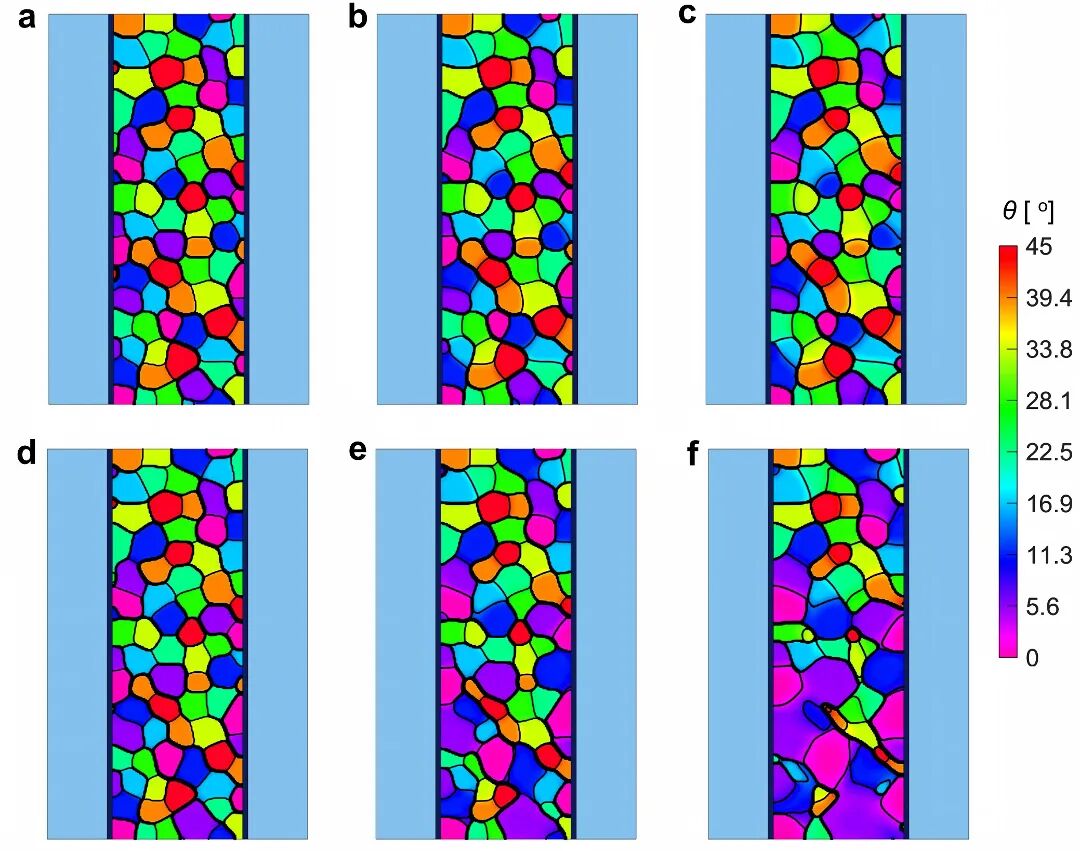
图2 | TSV中的晶粒演化。 a–c, 无热应力时10,000、25,000和50,000 s后的晶粒结构;d–f, 考虑热应力时10,000、25,000和50,000 s后的晶粒结构。
分析发现,取向角度接近0°的晶粒逐渐长大,而接近45°的晶粒不断缩小,使TSV中填充区域晶粒最终趋于沿[100]方向排列。研究表明,这与不同晶体取向晶粒所储存的弹性应变能有关:接近0°取向的晶粒虽然初始应变能较高,但其应变能在退火过程中下降更加明显,如图3d所示,因此在能量降低的过程中获得了生长优势。与此同时,晶粒演化还伴随着TSV填充区域平均杨氏模量下降以及TSV热应力的逐步释放。
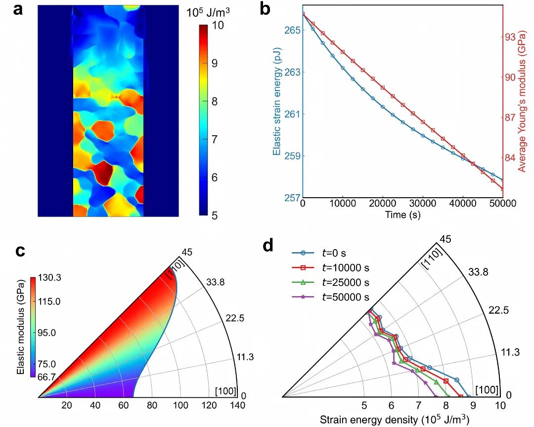
图3 | 热-应力耦合驱动晶粒演化的力学机制。 a, TSV中的应变能密度分布;b, 应变能和平均杨氏模量随时间的变化;c, Cu杨氏模量的取向依赖性;d, 不同取向晶粒中的应变能演化。
综上,这项研究揭示了热-应力耦合作用下TSV中晶粒演化与旋转的内在机制,阐明了热应力对晶粒尺寸与取向演化的影响。该研究为TSV可靠性分析及先进封装中的微结构与互连优化提供了理论参考。
Unraveling thermomechanical stress-driven grain evolution and rotation in through-silicon vias for advanced packaging¹
As artificial intelligence and high-performance computing continue to advance, 3D integrated circuits (3D ICs) are facing increasing demands for high-density vertical interconnects²-³. As through-silicon via (TSV) dimensions shrink, Cu filler may contain only a few grains, while crystallographic orientation and thermal stress caused by the Cu/Si coefficient of thermal expansion mismatch can significantly affect grain evolution and interconnect reliability⁴. Understanding the grain growth and rotation mechanisms driven by thermo-mechanical coupling is therefore important for optimizing TSV microstructure and performance.
As illustrated in Fig. 1, the Cu filler in a TSV consists of grains with different crystallographic orientations. In this work, a numerical framework coupling grain-boundary migration, grain rotation, and thermal stress was developed based on the Kobayashi–Warren–Carter model⁵, with orientation-dependent strain energy incorporated to describe grain evolution during annealing. As shown in Fig. 2, Cu grains mainly undergo coarsening without thermal stress, whereas thermal stress promotes grain growth and orientation rotation, leading to a preferential orientation.
Further analysis shows that grains with orientations close to 0° grow preferentially, while those near 45° shrink, resulting in grains preferentially aligned along the [100] direction. This behavior is associated with the evolution of orientation-dependent elastic strain energy, as shown in Fig. 3d. The findings reveal the mechanism of grain evolution and rotation under thermo-mechanical coupling and provide a theoretical reference for TSV reliability analysis and microstructural and interconnect optimization in advanced packaging.
参考文献
1. Jiang, H. et al. Unraveling thermomechanical stress-driven grain evolution and rotation in through-silicon vias for advanced packaging. Chip 5, 100176 (2026).
2. Hsiao, H.-Y. et al. Unidirectional growth of microbumps on (111)-oriented and nanotwinned copper. Science 336, 1007–1010 (2012).
3. Chen, Z. et al. Challenges and prospects for advanced packaging. Fundam. Res. 4, 1455–1458 (2024).
4. Liang, S. et al. Investigation of the interaction effect between the microstructure evolution and the thermo-mechanical behavior of Cu-filled through silicon via. IEEE Trans. Device Mater. Reliab. 22, 267–275 (2022).
5. Kobayashi, R., Warren, J. A. & Carter, W. C. A continuum model of grain boundaries. Phys. D: Nonlinear Phenom. 140, 141–150 (2000).
作者简介
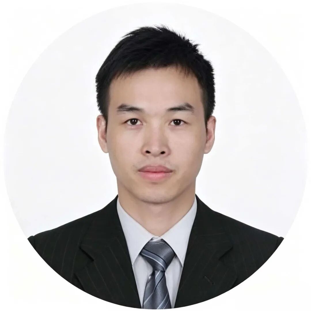
梁水保,合肥工业大学副教授,入选安徽省海外高层次人才计划。主要从事微电子封装与集成、元器件多场耦合行为及可靠性研究。以第一作者或通讯作者在IEEE Trans. Electron Devices、J. Appl. Phys.、IEEE Trans. Comput.-Aided Des. Integr. Circuits Syst.等学术期刊发表研究论文30余篇。
Dr. Shuibao Liang is an associate professor at Hefei University of Technology. He was selected for the Anhui Province Overseas High-Level Talent Program. His primary research interests include microelectronic packaging and integration, multiphysics coupling in electronic components, and reliability. He has authored over 30 research papers as the first or corresponding author in academic journals such as IEEE Trans. Electron Devices, J. Appl. Phys., and IEEE Trans. Comput.-Aided Des. Integr. Circuits Syst.
论文链接:
https://www.sciencedirect.com/science/article/pii/S2709472325000577